Digital Logic Chapter 5 part 1 - Latches and Flip-flops
Digital Logic Chapter 5 part 1 - Latches and Flip-flops
Sequential Circuits
A sequential circuit consists of a combinational circuit to which storage elements are connected to form a feedback path.
The binary information stored in the memory elements at any given time defines the state of the sequential circuits.
$(inputs, current State)$ $\Longrightarrow$ $(outputs, next State)$, the behavior is specified by a time sequence of inputs and internal states.
Synchronous Sequential Circuits
A system whose behavior can be defined from the knowledge of its signals at discrete instants of time.
Usually achieved by a timing device: clock generator, which means the outputs are affected only with the application of a clock pulse.
Asynchronous Sequential Circuits
A system whose behavior depends upon input signals at any instant of time and the order in which the inputs change.
Commonly used storage devices are time-delay devices, and the propagation delay of the logic gates (time-delay devices) provides the required storage.
Can be viewed as combinational circuit with feedback, and can be unstable at times
Storage Elements
State: all the information about a circuit necessary to explain its future behavior
Latch
SR Latch
SR Latch
It stores 1 bit of infomation, consists of two cross-coupled NOR gates or NAND gates.
Two input signals: $set(S)/Reset(R)$
Two output signals: $Q/Q’$
Two useful states: $setState(Q=1,Q’=0)/resetState(Q=0,Q’=1)$
Note: $Q$ and $Q’$ should always be different. And $(S,R)$ should go back to $(0,0)$ before any other changes to avoid the occurrence of the undefined state.
Consider 4 possible cases:
1.$S=1,R=0$ $\Longrightarrow$ $Q=1,Q’=0$ Set the output.
2.$S=0,R=1$ $\Longrightarrow$ $Q=0,Q’=1$ Reset the output.
3.$S=0,R=0$ $\Longrightarrow$ $Q=Q{prev},Q’=Q’{prev}$ Memory function.
4.$S=1,R=1$ $\Longrightarrow$ $Q=0,Q’=0$ Forbidden invalid state.
| $S$ | $R$ | $Q$ | $Q’$ | $State$ |
|---|---|---|---|---|
| 0 | 0 | $Q_{prev}$ | $Q’_{prev}$ | Memory |
| 0 | 1 | 0 | 1 | Reset |
| 1 | 0 | 1 | 0 | Set |
| 1 | 1 | 0 | 0 | Forbidden |
S’R’ Latch with NAND gates
Low active Set/Reset inputs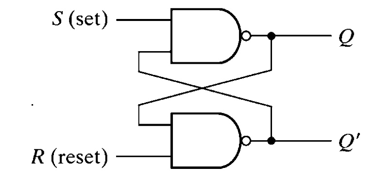
| $S$ | $R$ | $Q$ | $Q’$ | $State$ |
|---|---|---|---|---|
| 0 | 0 | 1 | 1 | Forbidden |
| 0 | 1 | 1 | 0 | Set |
| 1 | 0 | 0 | 1 | Reset |
| 1 | 1 | $Q_{prev}$ | $Q’_{prev}$ | Memory |
Clocked SR Latch
Use Clock (or En) to enable/disable the SR latch
$C=0$, no change(disabled)
$C=1$, operates as normal SR latch (enabled)
| $C$ | $S$ | $R$ | $Q$ | $Q’$ | $State$ |
|---|---|---|---|---|---|
| 0 | X | X | $Q_{prev}$ | $Q’_{prev}$ | no change |
| 1 | 0 | 0 | $Q_{prev}$ | $Q’_{prev}$ | Memory |
| 1 | 0 | 1 | 0 | 1 | Reset |
| 1 | 1 | 0 | 1 | 0 | Set |
| 1 | 1 | 1 | 0 | 0 | Forbidden |
D Latch
It stores 1 bit of infomation, constructed from a gated SR latch by connecting the D input to S input and D’ to R, which makes sure S and R are different in the SR Latch.
Two input signals: $Clock(clk/En)/Data(D)$
Two output signals: $Q/Q’$
Note: avoid invalid cases in SR Latches.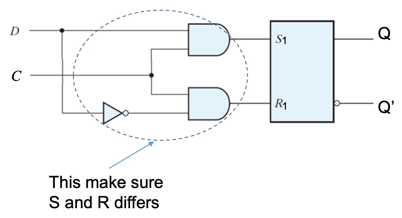
.jpeg)
| $C$ | $D$ | $Q$ | $Q’$ | $State$ |
|---|---|---|---|---|
| 0 | X | $Q_{prev}$ | $Q’_{prev}$ | no change(Memory) |
| 1 | 0 | 0 | 1 | Q follows D |
| 1 | 1 | 1 | 0 | Q follows D |
Flip-flop
Trigger
Level sensitive
The state transition starts as soon as the clock is during logic 1 (positive level-sensitive) or logic 0 (negative level-sensitive) level.
Edge triggered
The state transition starts only at positive (positive edge-triggered) or negative edge (negative edge-triggered) of the clock signal.
D Flip-flop
Standard DFF Properties
Inputs: $Clk$,$D$
A D flip-flop is formed by two separate latches:
A master D latch (negative level sensitive)
A slave D latch (positive level sensitive)
Positive-edge-triggered D flip-flop:
When $CLK = 0$:
master is transparent
slave is opaque
D passes through to P
When $CLK = 1$
master is opaque
slave is transparent
P passes through to Q
Thus, on the rising edge of the clock ($CLK$ rises from 0$\rightarrow$1)
D passes through to Q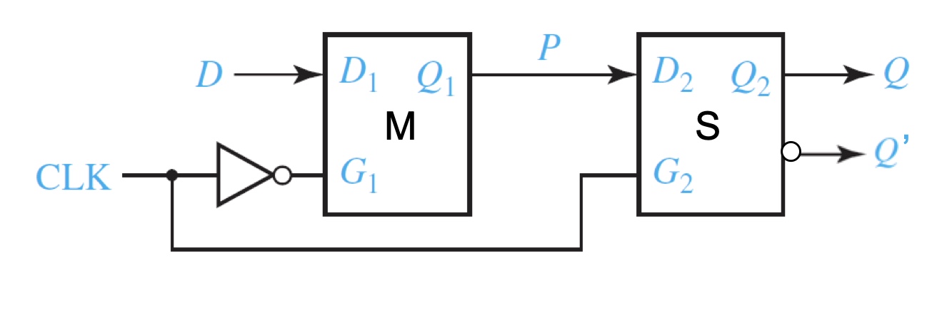
| $C$ | $D$ | $Q$ | $Q’$ | $State$ |
|---|---|---|---|---|
| 0 | X | $Q_{prev}$ | $Q’_{prev}$ | no change |
| 1 | X | $Q_{prev}$ | $Q’_{prev}$ | no change |
| $\uparrow$ | 0 | 0 | 1 | Q follows D |
| ↑ | 1 | 1 | 0 | Q follows D |
Setup time and hold time
Setup time
D input must be maintained at a constant value prior to the application of the positive Clk pulse
Hold time
Data input must not change after the application of the positive Clk pulse
DFF with Reset
Active low reset
$Reset = 0$: Q is forced to 0
$Reset = 1$: flip-flop behaves as ordinary D flip-flop
| $R$ | $C$ | $D$ | $Q$ | $Q’$ | $State$ |
|---|---|---|---|---|---|
| 0 | X | X | 0 | 1 | Reset on power, forced $Q = 0$ |
| 1 | $\uparrow$ | 0 | 0 | 1 | Q follows D |
| 1 | $\uparrow$ | 1 | 1 | 0 | Q follows D |
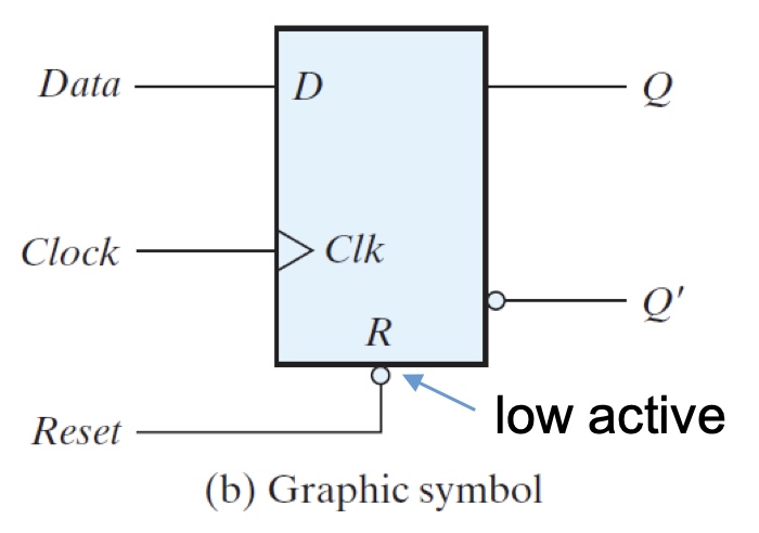
The state of FFs are unknown when power is on. A direct input can force the FFs to a known state before the system starts.
E.g. when $Reset = 1$, FF’s output is forced to 0
Synchronous vs. asynchronous resettable Flip Flop
Asynchronous: resets immediately when $Reset = 1$
Synchronous: resets at the clock edge only
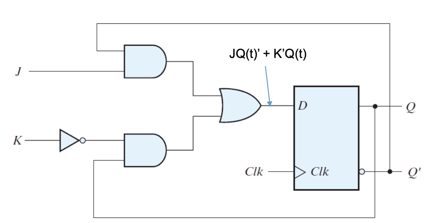
J-K Flip-flop
e.g. Positive edge-triggered JKFF
At rising edge of clock
$J = K = 0$, Q is unchanged
$J = K = 1$, Q toggles
$J = 1, K = 0$, Q is set to 1
$J = 0, K = 1$, Q is reset to 0
Characteristic equation:
T Flip-flop
T: Toggle
$T = 0$, a clock edge does not change the output.
$T = 1$, a clock edge complements the output.
Useful for designing binary counters.
| $T$ | $Q_{next}$ | $State$ |
|---|---|---|
| 0 | $Q$ | no change |
| 1 | $Q’$ | take $Q$’s complement |
Characteristic equation:

Characteristic Table
Characteristic table: describe the behavior of a flip-flop based on its input and current state Q(t) just before the rising edge of the clock, and the resulting next state Q(t+1) after the clock transition.
Characteristic equation: derived from the Characteristic table, e.g. $Q_{t+1} = D$
- From characteristic table to truth table
- Algebrically or using K-map to get characteristic equation

