Digital Logic Chapter 5 part 2 - Synchronous Sequential Logic
Digital Logic Chapter 5 part 2 - Synchronous Sequential Logic
Analysis of Sequential Circuits
Ways to describe a digital circuit
logic diagram (逻辑电路图): graphical representation of a digital circuit that uses standard symbols
K-map (卡诺图): graphical representation of a logic function used to simplify Boolean expressions
function table (功能表)(truth table): list of all possible input combinations and the corresponding output values for a given logic function
characteristic equations (特征方程): Describe the behavior of a sequential logic circuit, the next state is defined as a function of the inputs and the present state
excitation/input equation (激励方程): Defines the part of the circuit that generates the inputs to sequential logic circuit
state table (状态表): tabular representation of a sequential logic circuit that shows the current state, input, next state, and output for all possible input combinations
state equation (次态方程): defines the next state of a sequential logic circuit based on the current state and input values
state diagram (状态图): graphical representation of a sequential logic circuit that shows the states, transitions, and input-output relationships
Analysis Procedure of Clocked Sequential Circuits
Steps:
- Derive excitation/input equations for FF inputs
- Derive state and output equations
Substitute the excitation equations into the flip-flop characteristic equations to obtain next state equations.
Determine the output equations according current state and input - Generate state and output tables
- Generate state diagram
Important: FF’s Characteristic equation:
DFF $Q(t+1) = D(t)$
JKFF $Q(t+1) = J(t)Q(t)’ + K(t)’Q(t)$
TFF $Q(t+1) = T(t)’Q(t) + T(t)Q(t)’$
Example 1 using DFF $Q(t+1) = D(t)$:
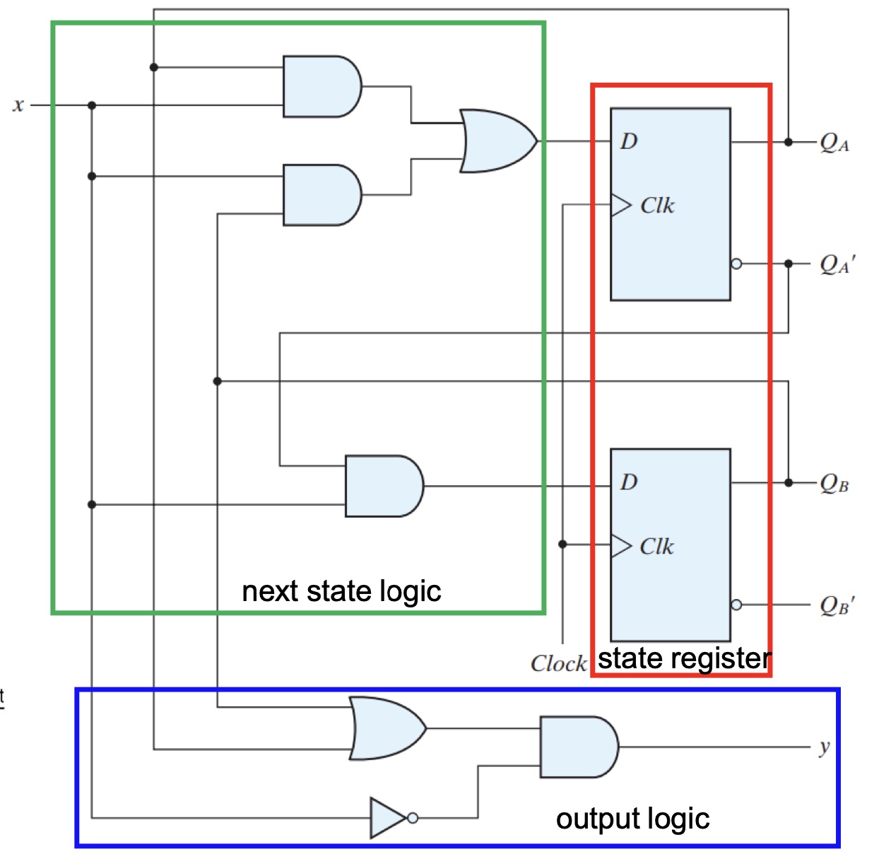
- Derive excitation/input equations for FF inputs
$D_A = Q_Ax + Q_Bx$
$D_B = Q_A’x$ - State equation
$Q_A(t+1) = D_A(t)=Q_Ax + Q_Bx$
$Q_B(t+1) = D_B(t) = Q_A’(t)x(t)$ - Output equation
$y(t) = (Q_A(t) + Q_B(t))x’(t)$
All signals are labeled by t, thus $y = (Q_A + Q_B)x’$ - Generate state and output tables
| Present state | Present state | Input | Next state | Next state | Output |
|---|---|---|---|---|---|
| $Q_A$ | $Q_B$ | $x$ | $Q_{Anext}$ | $Q_{Bnext}$ | $y$ |
| 0 | 0 | 0 | 0 | 0 | 0 |
| 0 | 0 | 1 | 0 | 1 | 0 |
| 0 | 1 | 0 | 0 | 0 | 1 |
| 0 | 1 | 1 | 1 | 1 | 0 |
| 1 | 0 | 0 | 0 | 0 | 1 |
| 1 | 0 | 1 | 1 | 0 | 0 |
| 1 | 1 | 0 | 0 | 0 | 1 |
| 1 | 1 | 1 | 1 | 0 | 0 |
Generate state diagram
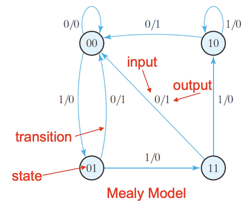
Example 2 using JKFF $Q(t+1) = J(t)Q(t)’ + K(t)’Q(t)$:
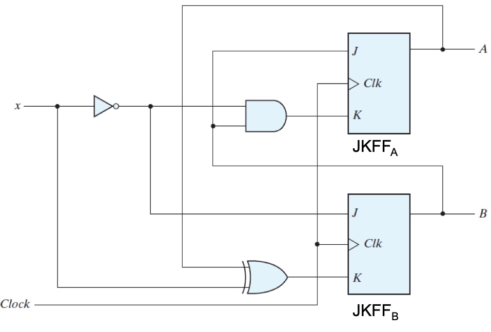
Derive excitation/input equations for FF inputs
$J_A = B$
$K_A= Bx’$
$J_B=x’$
$K_B=A \oplus x$State equation
$A(t+1) = J_AA’ + K_A’A= BA’ + (Bx’)’A$
$B(t+1) = J_BB’ + K’_BB=B’x’ +(A \oplus x)’B $No extra output equations
Generate state and output tables
| Present state | Present state | Input | Next state | Next state | FF inputs | FF inputs | FF inputs | FF inputs |
|---|---|---|---|---|---|---|---|---|
| $A$ | $B$ | $x$ | $A_{next}$ | $B_{next}$ | $J_A$ | $K_A$ | $J_B$ | $K_B$ |
| 0 | 0 | 0 | 0 | 1 | 0 | 0 | 1 | 0 |
| 0 | 0 | 1 | 0 | 0 | 0 | 0 | 0 | 1 |
| 0 | 1 | 0 | 1 | 1 | 1 | 1 | 1 | 0 |
| 0 | 1 | 1 | 1 | 0 | 1 | 0 | 0 | 1 |
| 1 | 0 | 0 | 1 | 1 | 0 | 0 | 1 | 1 |
| 1 | 0 | 1 | 1 | 0 | 0 | 0 | 0 | 0 |
| 1 | 1 | 0 | 0 | 0 | 1 | 1 | 1 | 1 |
| 1 | 1 | 1 | 1 | 1 | 1 | 0 | 0 | 0 |
- Generate state diagram
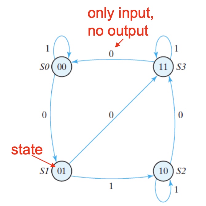
Example 3 using TFF $Q(t+1) = T(t)’Q(t) + T(t)Q(t)’$:
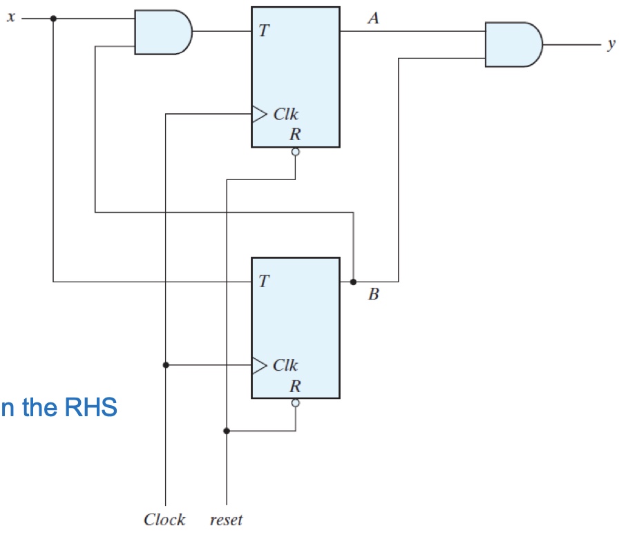
Derive excitation/input equations for FF inputs
$T_A = Bx$
$T_B = x$State equation
$A(t+1) = T_A \oplus Q_A = (Bx) \oplus A$
$B(t+1)=T_B \oplus Q_B = x \oplus B$Output equation
$y = AB$Generate state and output tables
| Present state | Present state | Input | Next state | Next state | Output |
|---|---|---|---|---|---|
| $A$ | $B$ | $x$ | $A_{next}$ | $B_{next}$ | $y$ |
| 0 | 0 | 0 | 0 | 0 | 0 |
| 0 | 0 | 1 | 0 | 1 | 0 |
| 0 | 1 | 0 | 0 | 1 | 0 |
| 0 | 1 | 1 | 1 | 0 | 0 |
| 1 | 0 | 0 | 1 | 0 | 0 |
| 1 | 0 | 1 | 1 | 1 | 0 |
| 1 | 1 | 0 | 1 | 1 | 1 |
| 1 | 1 | 1 | 0 | 0 | 1 |
- Generate state diagram
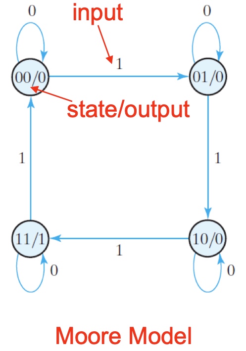
Finite State Machine
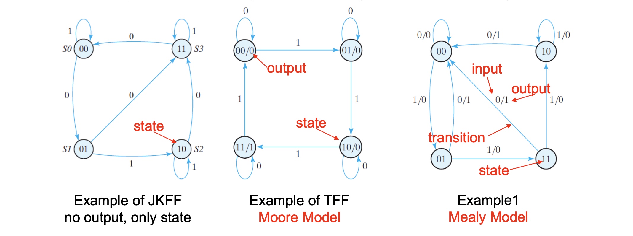
A synchronous sequential circuit can be modeled by FSM.
State register $𝑞(t+1) = 𝑞_{next}(t)$
Stores current state
Loads next state at clock edge
Combinational logic
Computes next state (next state logic $h: x × 𝑞 → 𝑞_{𝑛𝑒𝑥𝑡}$ )
Computes outputs
output logic $f: x × 𝑞 → 𝑦$ (Mealy machine, with blue line)
or $f: 𝑞 → 𝑦$ (Moore machine, without blue line)

Two types of finite state machines differ in output logic:
Moore FSM: outputs depend only on current state
Mealy FSM: outputs depend on current state and inputs, to synchronize a Mealy circuit, the inputs must be synchronized with the clock and the outputs must be sampled immediately before the clock edge
State Minimization & Encoding
State minimization
Reductions on the number of flip-flops (states) and the number of gates.
For an FSM with m states, we need $log_2m$ FFs.
Reduction steps
- Find rows in the state table that have identical next state and output entries. They correspond to equivalent states. If there are no equivalent states, stop.
- When 2 states are equivalent, one of them can be removed. Update the entries of the remaining table to cancel the removed state. Go to 1.
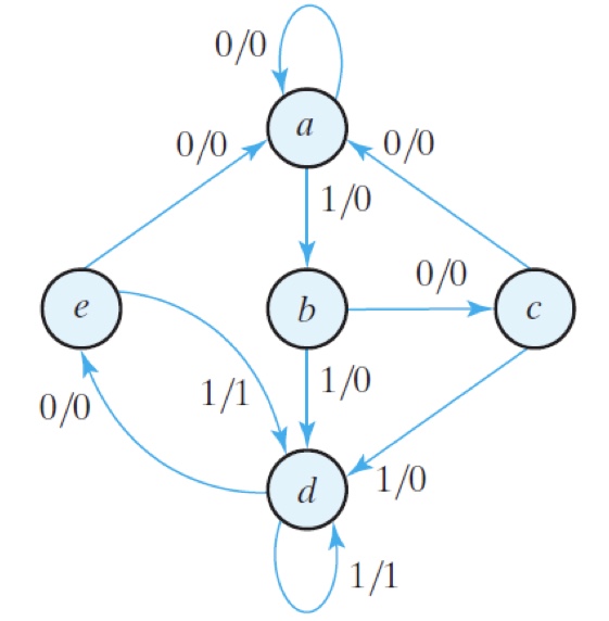
Example: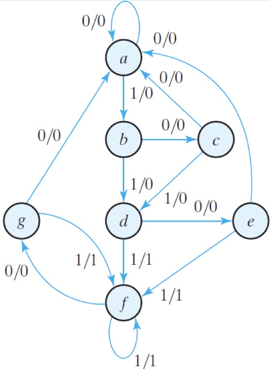 $\longrightarrow$
Start table:
| Present state | Next state | Next state | Output | Output |
|---|---|---|---|---|
| $x=0$ | $x=1$ | $x=0$ | $x=1$ | |
| a | a | b | 0 | 0 |
| b | c | d | 0 | 0 |
| c | a | d | 0 | 0 |
| d | e | f | 0 | 1 |
| e | a | f | 0 | 1 |
| f | g | f | 0 | 1 |
| g | a | f | 0 | 1 |
1st turn: $e \equiv g$
| Present state | Next state | Next state | Output | Output |
|---|---|---|---|---|
| $x=0$ | $x=1$ | $x=0$ | $x=1$ | |
| a | a | b | 0 | 0 |
| b | c | d | 0 | 0 |
| c | a | d | 0 | 0 |
| d | e | f | 0 | 1 |
| e | a | f | 0 | 1 |
| f | f | 0 | 1 |
2nd turn: $d \equiv f$
| Present state | Next state | Next state | Output | Output |
|---|---|---|---|---|
| $x=0$ | $x=1$ | $x=0$ | $x=1$ | |
| a | a | b | 0 | 0 |
| b | c | d | 0 | 0 |
| c | a | d | 0 | 0 |
| d | e | 0 | 1 | |
| e | a | 0 | 1 |
Encoding(assign binary state to the states)
Different state encodings (assignments) result in different circuits for the intended FSM.
There is no easy state-encoding procedure that guarantees a minimal-cost or minimum-delay combinational circuits
Exploration of all possibilities are impossible.
Heuristic are often used.
Binary counting
Minimum-bit change
One-hot encoding
Design of Sequential Circuits
Design Procedure of Sequential Circuits
- Specification: design description or timing diagram
- Formulation: develop state diagram
- Generate state and output tables
- Minimize States if necessary
- Assign binary values to the state (encoding)
- Derive state and output equations
- Choose memory elements (DFFs, JKFFs, TFFs)
- Derive simplified excitation/input equations and output equations
- Draw logic schematic
Choice of Memory Elements
Given the state transition table, we wish to find the FF input conditions that will cause the required transition.
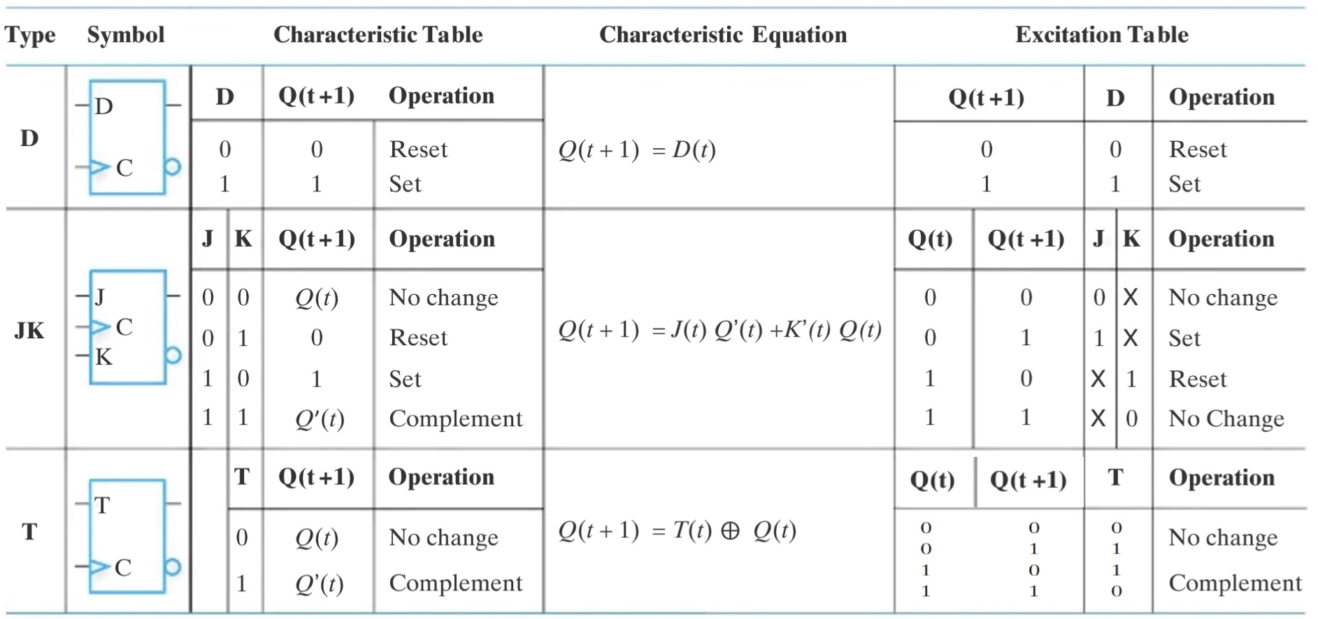
A tool for such a purpose is the excitation table, which can be derived from the characteristic table/equation.
D FFs are good for applications requiring data transfer (shift registers).
T FFs are good for those involving complementation (binary counters).
Many digital systems are constructed entirely with JK FFs because they are the most versatile available.
FF’s Excitation Table
Design Example: Design with DFF: A Sequence Detector
Detect three consecutive 1’s in a string of bits (using Moore machine, overlapping)
If detected, output=1; otherwise output=0State diagram
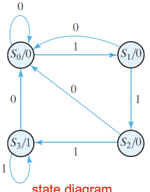
State and output table
| Present state | Next state | Next state | Output | Output |
|---|---|---|---|---|
| $S(AB)$ | $x=0$ | $x=1$ | $x=0$ | $x=1$ |
| $S_0 (00)$ | $S_0$ | $S_1$ | 0 | 0 |
| $S_1(01)$ | $S_0$ | $S_2$ | 0 | 0 |
| $S_2(10)$ | $S_0$ | $S_3$ | 0 | 0 |
| $S_3(11)$ | $S_0$ | $S_3$ | 1 | 1 |
No need for simplification
State assignment in 3
Derive state and output equations
| $A(t)$ | $B(t)$ | $x$ | $A(t+1)$ | $B(t+1)$ | $y$ |
|---|---|---|---|---|---|
| 0 | 0 | 0 | 0 | 0 | 0 |
| 0 | 0 | 1 | 0 | 1 | 0 |
| 0 | 1 | 0 | 0 | 0 | 0 |
| 0 | 1 | 1 | 1 | 0 | 0 |
| 1 | 0 | 0 | 0 | 0 | 0 |
| 1 | 0 | 1 | 1 | 1 | 0 |
| 1 | 1 | 0 | 0 | 0 | 1 |
| 1 | 1 | 1 | 1 | 1 | 1 |
$A(t+1)=D_A(A(t),B(t),x)=\Sigma(3,5,7)$
$B(t+1)=D_B(A(t),B(t),x)=\Sigma(1,5,7)$
$y(A,B,x)=\Sigma(6,7)$
Choose DFFs
2 bits encoding leads to 2 DFFs.
$A(t+1) =D_A(t)$
$B(t+1)=D_B(t)$Derive simplified excitation/input equations and output equations

$D_A=Ax+Bx$
$D_B=Ax+B’x$
$y=AB$Logic schematic(Omitted)
